This is a practical guide to Surface Science for researchers working in the Semiconductors Industry.
Dans ce tout nouveau guide, vous apprendrez tout sur :
Plongeons dans le vif du sujet.
Semiconductor manufacturers face the constant challenge of maximizing performance and refining processes. Often underestimated, surface properties play a crucial role in optimizing these performances. By measuring these properties, we gain valuable insights into material properties, processes, and device performance, ultimately leading to:

We use the following surface properties to understand the behavior of Semiconductors products and improve their quality.
Sample Image taken from Droplet Lab Tensiometer.
Young – Méthode Laplace
Méthode polynomiale
Ideally, when we place a drop on a solid surface, a unique angle exists between the liquid and the solid surface. We can calculate the value of this ideal contact angle (the so-called Young’s contact angle) using Young’s equation. In practice, due to surface geometry, roughness, heterogeneity, contamination, and deformation, the contact angle value on a surface is not necessarily a single consistent value but rather falls within a range. The upper and lower limits of this range are known as the advancing and receding contact angles, respectively. The values of advancing and receding contact angles for a solid surface are highly sensitive to many parameters, such as temperature, humidity, homogeneity, and minor contamination of the surface and liquid. For example, the advancing and receding contact angles of a surface can differ at different locations.
Les surfaces et les revêtements pratiques présentent naturellement une hystérésis d’angle de contact, indiquant une gamme de valeurs d’équilibre. Lorsque nous mesurons les angles de contact statiques, nous obtenons une seule valeur dans cette plage. S’appuyer uniquement sur des mesures statiques pose des problèmes, tels qu’une mauvaise répétabilité et une évaluation incomplète de la surface en ce qui concerne l’adhérence, la propreté, la rugosité et l’homogénéité.
In practical applications, we need to understand how easily a liquid spreads (advancing angle) and how easily it is removed (receding angle), such as in painting and cleaning. Measuring advancing and receding angles offers a holistic view of liquid-solid interaction, unlike static measurements, which yield an arbitrary value within the range.
Ces informations sont cruciales pour les surfaces du monde réel avec des variations, une rugosité et une dynamique, aidant des industries telles que les cosmétiques, la science des matériaux et la biotechnologie à concevoir des surfaces efficaces et à optimiser les processus.
Découvrez comment la mesure de l’angle de contact est effectuée sur notre tensiomètre
Pour une compréhension plus complète de la mesure de l’angle de contact, lisez notre mesure de l’angle de contact : le guide définitif
These reference measurements show how deionized water wets four standard substrates measured with the Droplet Lab Dropometer. Use them as visual and numerical benchmarks when you're checking your own sample preparation, treatments, and chemistry.
Full contact angle and surface energy datasets (including additional liquids and statistics) are available on our dataset hub.
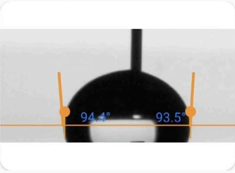
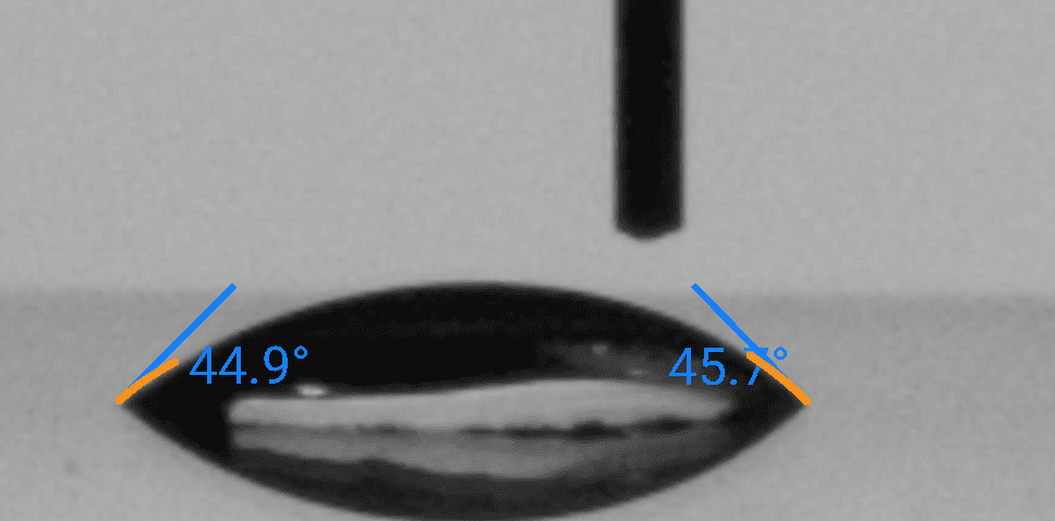
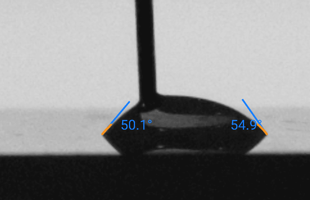
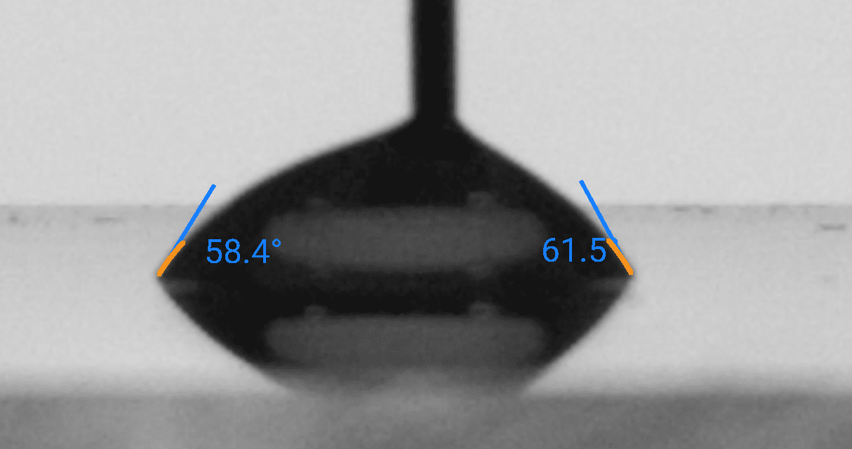
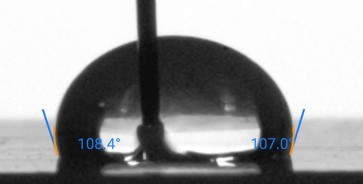
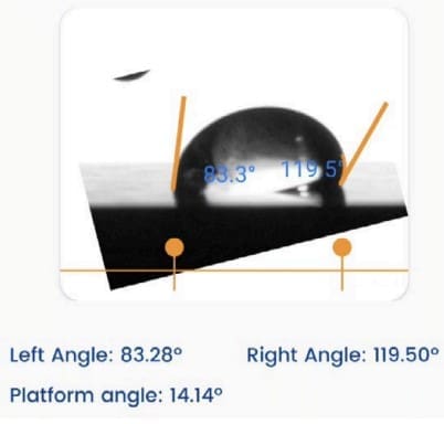
The droplet images above are taken from the same benchmark series as our open dataset. For each substrate and probe liquid we report:
● Advancing and receding contact angles (and hysteresis)
● Derived surface energy (SFE) values based on multi-liquid measurements
● Measurement conditions, uncertainties, and sample preparation details
Comparing your own droplet shapes and angles against these references is a fast way to spot contamination, treatment drift, or unexpected changes in wettability.
Measurements were performed with the Droplet Lab Dropometer under controlled laboratory conditions. Treat these values as sanity checks and starting points for your own process targets, not as product specifications.
Cette propriété mesure la force qui agit à la surface d’un liquide, dans le but de minimiser sa surface.
Sample Image taken from Droplet Lab Tensiometer
Tension superficielle dynamique
La tension superficielle dynamique diffère de la tension superficielle statique, qui fait référence à l’énergie de surface par unité de surface (ou à la force agissant par unité de longueur le long du bord d’une surface liquide).
La tension superficielle statique caractérise l’état d’équilibre de l’interface liquide, tandis que la tension superficielle dynamique tient compte de la cinétique des changements à l’interface. Ces changements peuvent impliquer la présence de tensioactifs, d’additifs ou de variations de température, de pression et de composition à l’interface.
Quand utiliser la mesure dynamique de la tension superficielle
Dynamic surface tension is essential for processes that involve rapid changes at the liquid-gas or liquid-liquid interface, such as droplet and bubble formation, coalescence (change in surface area), the behavior of foams, and the drying of paints (change in composition, e.g., evaporation of solvent). It is measured by analyzing the shape of a hanging droplet over time.
La tension superficielle dynamique s’applique à diverses industries, notamment les cosmétiques, les revêtements, les produits pharmaceutiques, la peinture, l’alimentation et les boissons, ainsi que les processus industriels, où la compréhension et le contrôle du comportement des interfaces liquides sont essentiels pour la qualité du produit et l’efficacité des processus.
Apprenez comment la mesure de la tension superficielle est effectuée sur notre tensiomètre
Pour une compréhension plus complète de la mesure de l’énergie de surface, lisez notre mesure de la tension superficielle : le guide définitif
Sample Image taken from Droplet Lab Tensiometer
Découvrez comment la mesure de l’énergie de surface est effectuée sur notre tensiomètre
Pour une compréhension plus complète de la mesure de l’énergie de surface, lisez notre mesure de l’énergie de surface : le guide définitif
For benchmark contact angle and surface energy values on glass, nylon, PMMA, and Teflon, see the Open Benchmark Data panel above or visit our Dataset Hub for full CSV downloads.
L’angle de glissement mesure l’angle auquel un film liquide glisse sur une surface solide. Il est couramment utilisé pour évaluer la résistance au glissement d’une surface.
Sample Image taken from Droplet Lab Tensiometer
Apprenez comment la mesure de l’angle de glissement est effectuée sur notre tensiomètre
Pour une compréhension plus complète de la mesure de l’angle de glissement, lisez notre Mesure de l’angle de glissement : le guide définitif
Within the Semiconductors industry, several case studies exemplify the advantages of conducting surface property measurements.
In photolithography, meticulous pattern creation is key to manufacturing complex semiconductor devices. This process relies heavily on the delicate interplay between the photoresist and the substrate. Photoresist adhesion to the substrate acts as a linchpin, directly determining the sharpness and precision of the resulting patterns. To achieve optimal results, manufacturers delve into the surface science of these properties. By examining the substrate's surface energy and analyzing the contact angle exhibited by the photoresist, they gain valuable insights to fine-tune adjustments.
This refining process enhances adhesion properties, ultimately leading to a seamless pattern transfer. The benefits are manifold, including increased yields, sharper results, and a significant reduction in defects throughout the lithography process.

Chip packaging relies heavily on adhesives to securely bind the delicate semiconductor die to its protective casing. However, a major challenge arises from leftover adhesive residue, which can negatively impact device reliability.
To combat this issue, manufacturers meticulously measure and manage the sliding angle of the packaging material during application. This precise control ensures that the liquid adhesive smoothly glides away, leaving no unwanted residue behind. This optimization delivers two key benefits: firstly, it significantly reduces the risk of electrical shorts or unintended connections, and secondly, it effectively boosts the overall electrical performance of the device.

To achieve successful immersion lithography, meticulous management of the immersion fluid is crucial. A major failure point is the receding meniscus event, which leaves residual liquid behind on the wafer as a thin film or droplets. Ideally, the immersion fluid should be confined near the lens, allowing the wafer to scan smoothly during exposure.
For a semiconductor manufacturer, the meniscus failure mechanism remained a significant hurdle, hindering the successful implementation of immersion lithography. Recognizing the critical role of surface forces in drainage and pattern collapse during lithography, they sought a solution from a laboratory. The scientists, understanding the importance, developed a new fluid formulation with precisely tailored surface tension characteristics that facilitated proper liquid drainage, eliminating the meniscus issue.

Si vous êtes intéressé par la mise en œuvre de ces applications ou de toute autre application, veuillez nous contacter.
In an industry where precision reigns supreme, how can Semiconductors manufacturers ensure their products withstand scrutiny? The answer lies in standards and guidelines: the compass that guides them through the complex maze of quality and performance.
Standard practice for estimating a solid’s total surface free energy and separating it into dispersive and polar components by measuring sessile‑drop contact angles of two probe liquids (one polar, one non‑polar) of known surface tension on the surface. It is intended as a quantitative, comparative surface‑readiness metric for wetting/adhesion process control within an approximate applicable range of ~20–60 mN/m.
Use fixed‑time contact angles plus calculated γ components to confirm surface cleaning/treatment/priming is within a validated “pass band” before committing to downstream trials.
Trend γs,polar/γs,dispersive and spot‑to‑spot variability to diagnose under‑treatment, contamination, non‑uniform treatment, or material/lot shifts.
This method provides an image‑backed, quantitative surface‑readiness signal but does not by itself guarantee adhesion or print performance. Any pass/fail gates must be calibrated per material family + treatment recipe + ink/adhesive system by correlating D7490 outputs to your downstream KPI.
We hope this guide showed you how to apply surface science in the Semiconductors industry.
Maintenant, nous aimerions vous céder la parole :
Feel free to leave a comment below—we’d love to hear from you.